Radar PCBs are used in advanced driver assistance systems. They use tiny components and feature surface mount technology, which enables connections on all sides of the board. Surface mounting is also less expensive than through-hole mounting, making it an ideal choice for applications requiring dependability. Surface-mount components may also be smaller, allowing more components to be placed on a single circuit board.
RF PCB design software
A good RF PCB design software will offer many benefits for engineers. For example, it will support multiple platforms and allow multiple engineers and project stakeholders to share the same design data. RF-aware circuit simulation, embedded parasitic extraction, and frequency-dependent transmission-line models are all crucial to PCB design. It also offers export and import capabilities.
In addition, RF PCBs will need a special set of materials. As a result, RF PCBs require special design considerations, including a reduced mass. Additionally, RF Printed Circuit Boards will require specific scaling, as they will lose mass during the process of heat lamination.
RF PCBs are made from high-frequency materials and behave differently from standard PCBs. Therefore, it is important to understand the behavior of each material before scaling. If not, the result will be improper layer performance and bad registration. With practice, you can set a consistent scale factor for each material and use it to design future PCBs. However, you should remember that RF PCBs have very sensitive surfaces. If you have to prepare them with aggressive methods, you risk degrading the material. If you are unable to avoid significant deformation, your PCB will end up scrap.
Crosstalk is a common problem with RF PCBs. This problem tends to get worse the higher the density of the board. To combat this problem, you need to choose the right materials for your PCB. Microstrip is the best option for this, but it is also necessary to choose the correct transmission lines.
As wireless technology spreads from smartphones and tablets to wearables, it is imperative to have access to PCB design software. These tools will make the process of designing RF-centric PCBs easier and faster. It will also reduce over-design margins and help designers collaborate with other teams.
RF PCBs are made to meet specific standards. By following these standards, manufacturers can produce high-quality designs and comply with relevant production procedures. One of these standards is CGMP, or Current, Good Manufacturing Practice regulations. CGMP regulations protect the consumer and ensure a high-quality product. They also regulate manufacturing processes and production facilities.
RF PCB design software should have tools that allow you to capture and export circuit details, including schematic symbols, in a standardized and easy-to-use manner. This allows you to avoid manual design entry and edits. The tool should also support automation, and should also have powerful scripting capabilities.
If you’re an engineer, it’s important to select a PCB design software that is compatible with your workflow. This will help you save time. Make sure that it includes features like schematic capture, bill of materials generation, and interactive routing. The software should also include training. You should also look for software that supports multiple planes, layers, and signals.
You must ensure that you have a clear objective and purpose when creating an RF PCB project. If you don’t, the manufacturer may cut components that don’t fit your specifications. The wrong components can cause flaws in your final product. If you’re outsourcing your RF PCB project, you should also ensure that you have complete confidence in your manufacturer.
Problems in RF PCB design
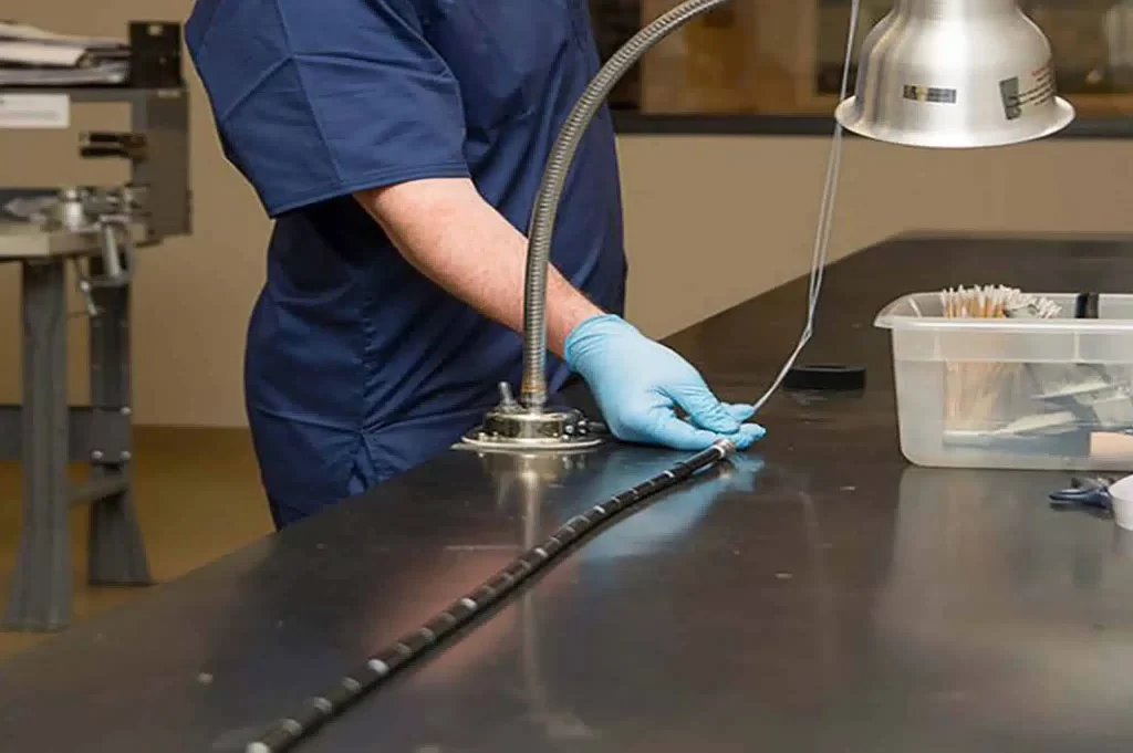
RF PCB design is not as simple as other types of electronic circuit design. This circuitry uses a complex network of conductive elements. During the layout process, RF PCB components may need to be modified. These changes can include repositioning pads, incorporating metal features, and changing the PCB footprint. These changes are usually done individually for individual components or base library parts. In addition, most traces must be manually added for specific RF topologies. This makes it imperative to set up design rules to ensure success.
One of the most important design considerations for RF PCBs is the impedance. Because high-frequency signals are susceptible to interference, it is important to use low-impedance traces. The characteristic impedance of these lines will depend on the type of material and the thickness of the layer. In general, values between 50 and 75 ohm are used for transmission lines. In addition, the traces should be short and smooth to reduce crosstalk.
Another important design consideration is component placement. Since RF circuitry typically requires tighter placement, RF circuit boards often contain more metal on the external layers. This can cause problems with PCB assembly. Further, the components on the board may be placed directly on the external layers. As a result, the layout of RF PCBs can be more complicated than a traditional one.
Other design considerations include skin effect, coupling effect, and distributed parameter circuit. These considerations should be considered during PCB layout to improve anti-interference performance. These considerations require careful planning and design. RF PCB design is different than other types of circuits, so it is vital to address these unique challenges.
Moisture is another important factor to consider. Moisture is a major contributor to temperature, and moisture affects RF performance. It can cause problems during high-frequency operations, so the designer should ensure that all layers of a laminate substrate are closely matched to each other. The Coefficient of Thermal Expansion (CTE) can also lead to functional failures, which is why it is essential to match CTEs across layers.
High-frequency circuitry tends to generate a lot of heat and should be cooled properly. This means that the materials used in RF PCB design should be low in coefficient of thermal expansion. Further, RF PCB design also requires careful consideration of the spacing between components. If this is not done, the resulting design will result in a poor-quality RF PCB.
Using an RF simulation tool is a good idea if you need to make a design that works in a range of frequencies. The Altium Designer simulation tool has many tools that can simulate circuits in various frequencies. It also allows you to easily send designs to EMI simulation tools like Ansys SIwave.
Applications for radar PCBs in advanced driver assistance systems
Radar-based ADAS systems provide a virtual sense of surroundings to assist drivers. These radars require high-frequency circuit materials with low dielectric constants. The Rogers Corporation offers high-quality radar PCBs for ADAS systems. Its products are used in many automotive applications.
Radar sensors are used by major American car manufacturers for ADAS features such as adaptive cruise control and emergency braking assistance. The radar-based technology also enables blind-spot monitoring in passenger cars and trucks with trailers. In 2018, the Dodge Ram 1500 introduced blind-spot monitoring based on this technology. In the same year, the company was awarded the FCA Supplier of the Year Award. The company has development sites in Santa Barbara, California, and Auburn Hills, Michigan.
Radar PCBs can be manufactured using the latest technology. A radar PCB has a high frequency laminate material on which an antenna is mounted. The RF circuit generates a radar lobe and the resulting signal is received by a separate RF circuit. This technology has an extended range, which allows for detection of objects far away. In addition, radar PCBs use a super-heterodyne processor to detect reflected signals.
Radar PCBs can be used in many applications. They are used in autonomous driving, intelligent lights, level meters, and other areas that require precision positioning. They are also used for radar sensors. They can be fabricated using a two-component injection molding process.
Radar PCBs are a critical component of ADAS. Their precision and flexibility make them an ideal choice for vehicles with ADAS technology. They can also be used to detect obstacles close to a vehicle. These sensors help prevent collisions. The information from these sensors can be incorporated into the navigation system to improve vehicle guidance.
Radar PCBs can also be used in driver vital-sign monitoring systems, which monitor vital signs. FMCW radars have a high resolution range and high-frequency range. These radars can measure the frequency of vibrations in objects. These radars are also used in touchless interfaces. A few examples of this technology include gesture-based door openers, gesture-based infotainment controls, and gesture-based remote controls. With their small dimensions, they can be easily integrated into the driver’s vehicle.
ADAS technology uses a wide variety of sensors. 77GHz radar sensors are widely used in active cruise control systems and can monitor the speed of vehicles ahead, the distance between two vehicles, and the speed of the car itself. Radar is expensive and may not be the best option for every application. Airborne lidar sensors are more efficient and cost-effective. These sensors send out laser pulses that reflect off of other objects. After a certain delay time, the distance from the other object can be calculated.
The automotive industry continues to add features and capabilities to the vehicles, including autonomous braking and adaptive cruise control. In some cases, these ADAS systems will become standard features. These new features are designed to enhance the experience and safety of the driver and others on the road.